 |
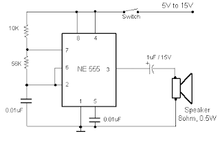
| Gbr. Skema Rangkaian Elektronic buzzer |
IC NE555
555 timer IC provides practical solutions and relatively inexpensive for a variety of electronic applications related to the timing (timing). Especially two of the most popular application is a series of monostable and astable timing.

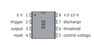
- Pin 1: Ground, is the input pin of the source of the negative DC voltage
- Pin 2: trigger, negative input from the lower comparators (comparator B) that maintain oscillation capacitor voltage in the lowest 1 / 3 Vcc and set RS flip-flop
- Pin 3: output, the output pin of the IC 555.
- Pin 4: reset, the pin that serves to reset the latch inside the IC to be influential to reset the IC work. This pin is connected to a PNP-type transistor gate, so the transistor will be active if given a logic low. Normally this pin is connected directly to Vcc to prevent reset
- Pin 5: control voltage, this pin serves to regulate the stability of the reference voltage negative input (comparator A). This pin can be left hanging, but to ensure the stability of the reference comparator A, usually associated with a capacitor of about 10nF to berorde pin groun
- Pin 6: threshold, this pin is connected to the positive input (comparator A) which will reset the RS flip-flop when the voltage on the capacitor from exceeding 2 / 3 Vc
- Pin 7: discharge, this pin is connected to an open collector transistor Q1 is connected to ground emitternya. Switching transistor serves to clamp the corresponding node to ground on the timing of certain
- Pin 8: vcc, pin it to receive a DC voltage supply. Usually will work optimally if given a 5-15V. the current supply can be seen in the datasheet, which is about 10-15mA.


 12:09 AM
 Unknown
 Posted in


0 comments:
Post a Comment