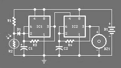
Anti-theft alarm circuit it produces an audible alarm when fridge is left open for a preset time.Rangkaian This versatile alarm is based on two 555 timer IC's. Both ICS are wired as astable Multivibrators.An LDR is connected in parallel to the timing capacitor
 |
| Skema Rangkaian Alarm anti maling |
C1 of IC 1.When is completely close door there will be no light inside the fridge and offers high resistance LDR R1 keeping fully charged.When door is left open, the lamp inside the fridge will remain glown, LDR will be illuminated, and its falls.This resistance makes
C1 stops charging and starts to discharge (In simple words, this is because at low resistance LDR bye passes much of the current in the parrallel path and capacitor gets less current). Now IC 1 starts oscillating
slightly and after a preset time of 25 ( time T1) seconds high.This its output goes out put makes the Ic 2 to produce oscillations and results in a beeping sound for next 20 (time T2) seconds and cycle is repeated till door is closed.
List Component alarm anti maling:
- R1: 10K 1/4W Resistance
- R3: 2.2 M 1/4W Resistance
- R4: 1M 1/4W Resistance
- C1: 10µF/25V Electrolytic Capacitance
- C2: 100nF/63V Polyester Capacitance
- D1: 1N4001 Diode
- IC1,IC2: NE 555 Timer ICs
- BZ1: Piezo Buzzer
- B1: 3V Cell
Note:
Assemble the circuit on a good quality PCB .Time T1 & T2 can be adjusted by varying C1, C2, R1, R4 etc (Refer data sheet of 555). Place the LDR close enough to the lamp inside the fridge.
IC 555 Pin No Designation Description

- Ground, is the input pin of the source of the negative DC voltage
- Trigger, negative input from the lower comparators (comparator B) that maintain oscillation capacitor voltage in the lowest 1 / 3 Vcc and set RS flip-flop
- Output, the output pin of the IC 555.
- Reset, the pin that serves to reset the latch inside the IC to be influential to reset the IC work. This pin is connected to a PNP-type transistor gate, so the transistor will be active if given a logic low. Normally this pin is connected directly to Vcc to prevent reset
- Control voltage, this pin serves to regulate the stability of the reference voltage negative input (comparator A). This pin can be left hanging, but to ensure the stability of the reference comparator A, usually associated with a capacitor of about 10nF to berorde pin groun
- Threshold, this pin is connected to the positive input (comparator A) which will reset the RS flip-flop when the voltage on the capacitor from exceeding 2 / 3 Vc
- Discharge, this pin is connected to an open collector transistor Q1 is connected to ground emitternya. Switching transistor serves to clamp the corresponding node to ground on the timing of certain
- Vcc, pin it to receive a DC voltage supply. Usually will work optimally if given a 5-15V. the current supply can be seen in the datasheet, which is about 10-15mA.


 7:46 PM
 Unknown
 Posted in


0 comments:
Post a Comment